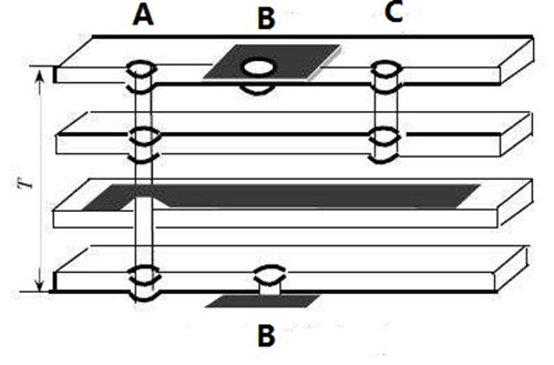
Let us first introduce the common holes in the PCB: through holes, blind holes, buried holes. The meaning and characteristics of these three holes.
Via, a common hole used to turn on or connect copper foil traces between conductive patterns in different layers of a board. For example (such as blind holes, buried holes), but can not be inserted into the component legs or other copper-plated holes for reinforcement. Because the PCB is formed by stacking many copper foil layers, each layer of copper foil is covered with an insulating layer so that the copper foil layers cannot communicate with each other, and the signal is linked by the via holes. (via), so there is a Chinese via hole.
The characteristic is: in order to meet the customer's demand, the through hole of the circuit board must be plugged, so that in the process of changing the traditional aluminum plug hole, the white plate is used to complete the surface resistance welding and plugging of the circuit board, so that the production is stable. The quality is reliable and the application is more perfect. The via holes mainly play the role of circuit interconnection and conduction. With the rapid development of the electronics industry, higher requirements are also placed on the manufacturing process and surface mount technology of printed circuit boards. The process of the via hole for plugging is applied, and the following requirements should be met: 1. There is copper in the via hole, and the solder resist plug can be plugged. 2. There must be tin-lead in the via hole. There is a certain thickness requirement (4um). There should be no solder-proof ink in the hole, resulting in hidden tin beads in the hole. 3. The via hole must have a solder mask ink plug hole, which is opaque, and must not have tin ring, solder ball and leveling requirements.
Blind hole: the outermost circuit in the PCB is connected to the adjacent inner layer by electroplating holes. Because it is not visible, it is called blind pass. At the same time, in order to increase the space utilization between PCB circuit layers, blind holes are applied. That is, a via hole to one surface of the printed board.
Features: The blind holes are located on the top and bottom surfaces of the board and have a certain depth for the link between the surface line and the underlying inner line. The depth of the hole usually does not exceed a certain ratio (aperture). This type of production requires special attention to the depth of the hole (Z-axis) to be just right. If you do not pay attention, it will cause difficulty in plating in the hole, so it is almost useless. You can also use the circuit layer that needs to be connected beforehand in the individual circuit layers. Drill the holes first, and finally glue them together, but you need a more precise positioning and alignment device.
Buried holes are links between any circuit layers inside the PCB but are not conducted to the outer layer, and are also meanings of via holes that do not extend to the surface of the board.
Features: In this process, it is impossible to use the method of drilling after bonding. It is necessary to perform drilling at the time of individual circuit layers. After the partial bonding of the inner layer, the first plating is performed first, and finally the bonding is completed, which is more than the original conduction. Holes and blind holes take more time, so the price is also the most expensive. This process is usually only used on high-density boards to increase the usable space of other circuit layers.
In the PCB production process, drilling is very important and should not be sloppy. Because the drilling is to drill the required vias on the copper clad plate to provide electrical connections and to fix the function of the device. If the operation is not proper, there is a problem in the process of the via hole, the device cannot be fixed on the circuit board, and the light influences the use, and the entire board is scrapped, so the drilling process is quite important.
Any question and inquiry, please contact [email protected] for your answer.
Thank you.
Engineer from Winco-PCB